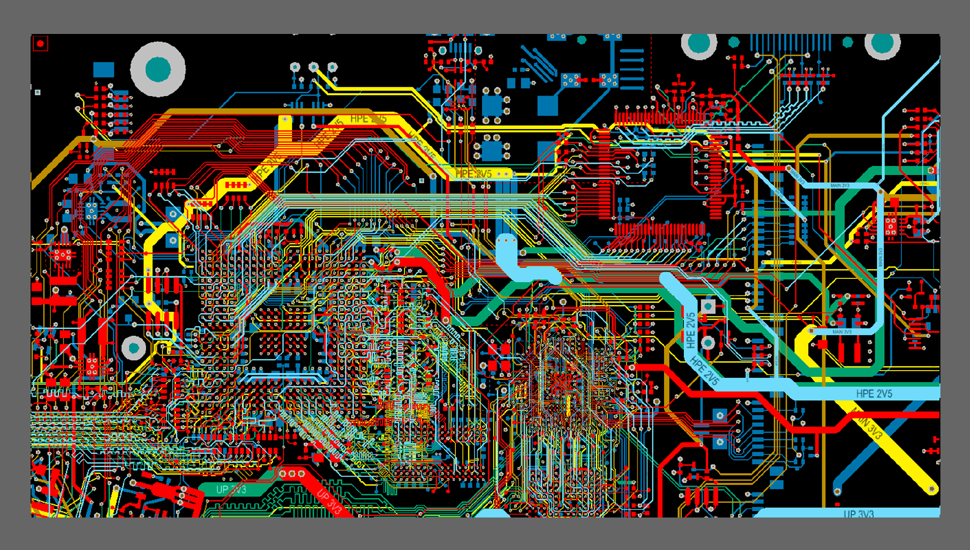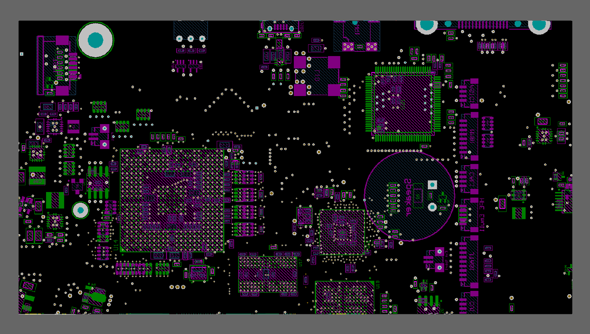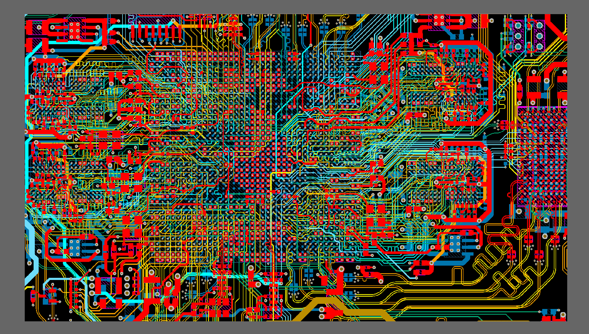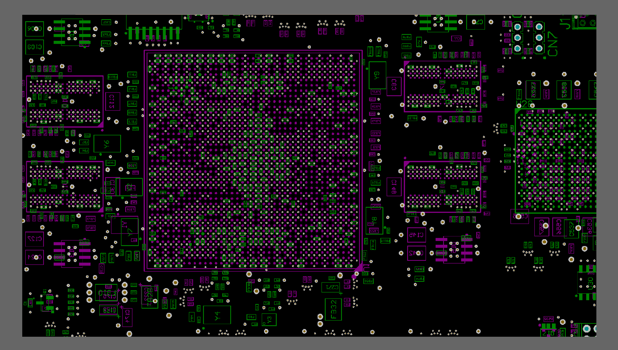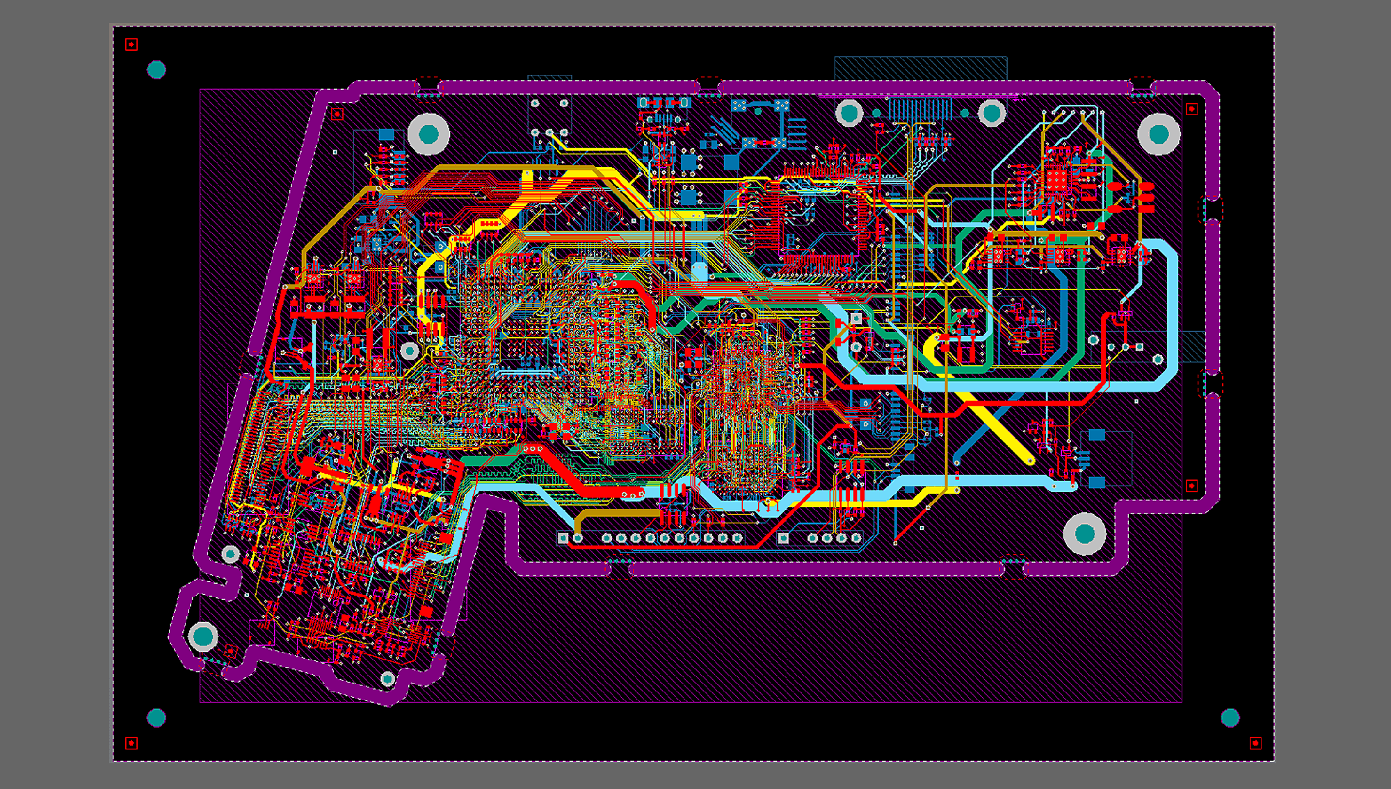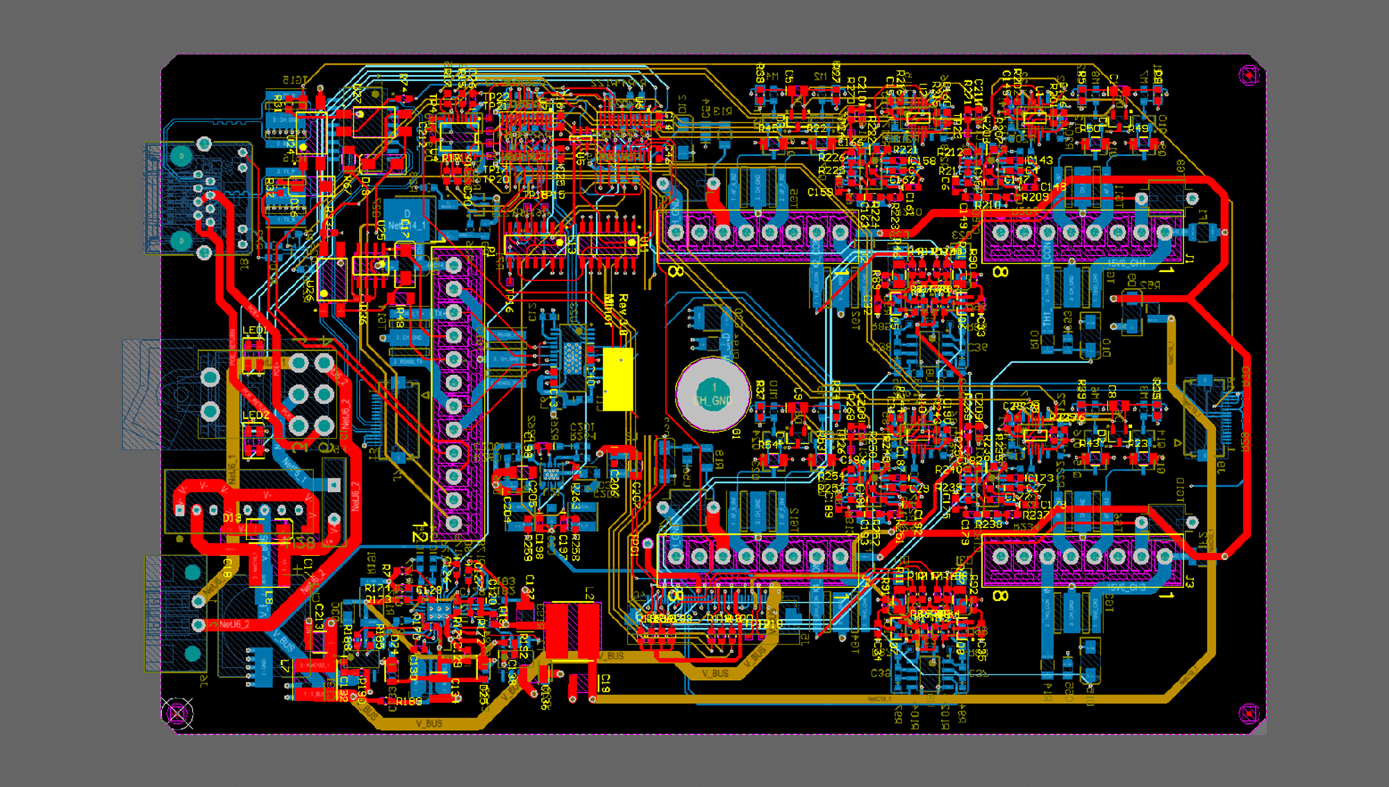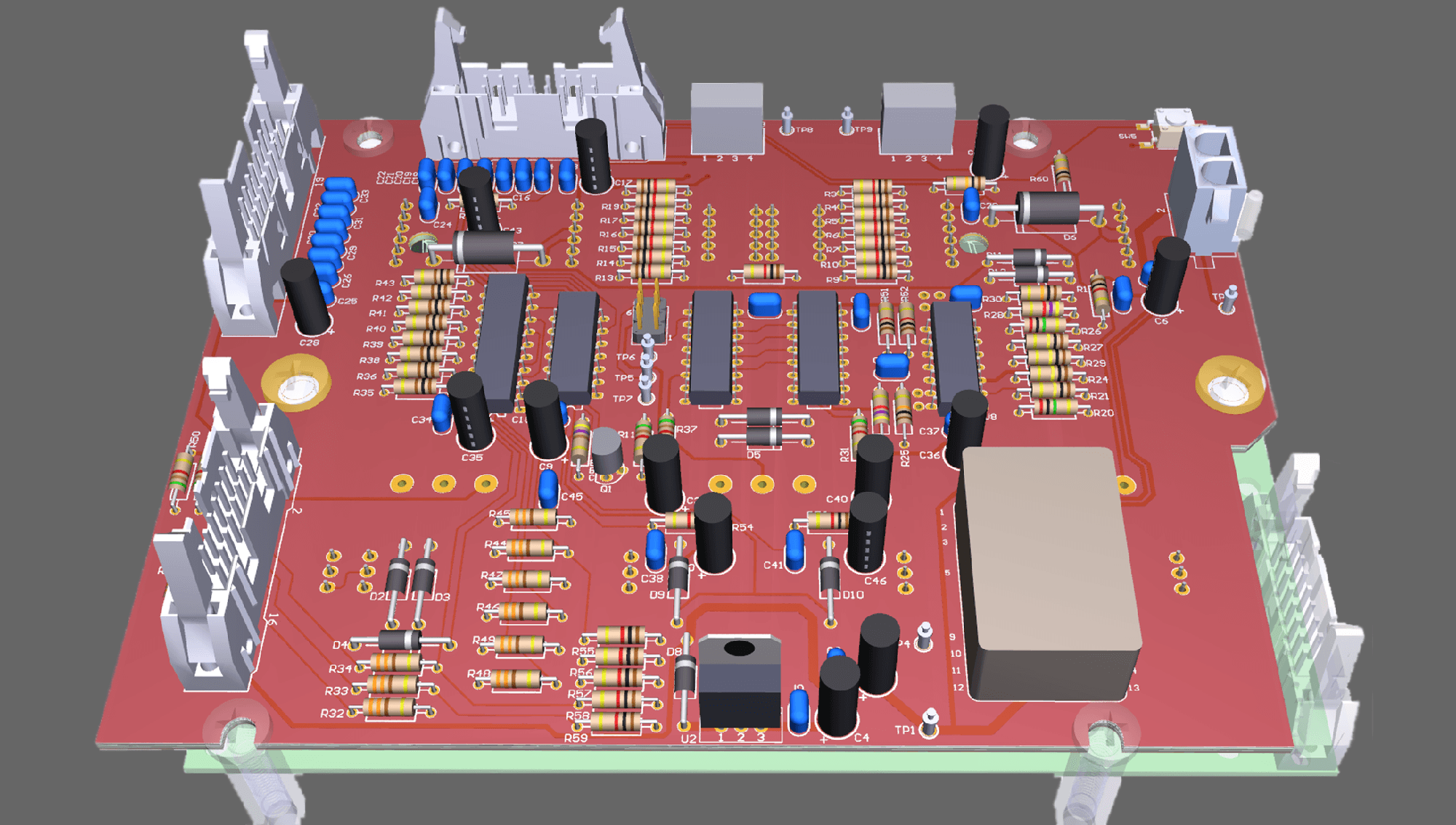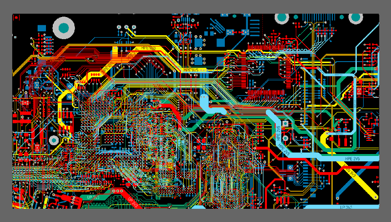
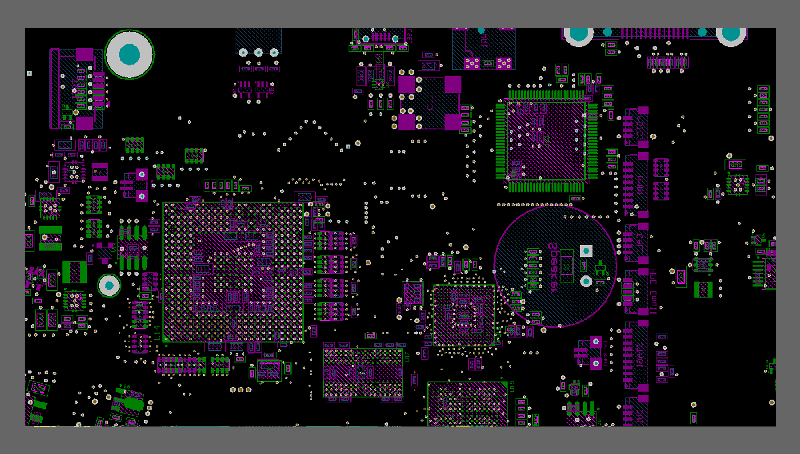
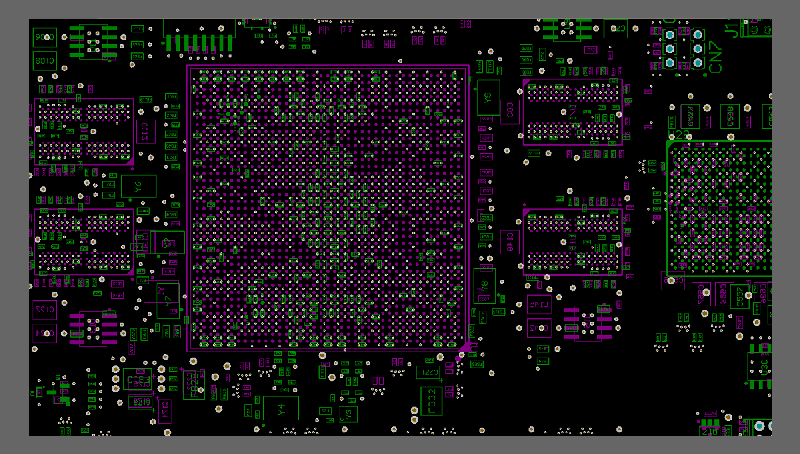
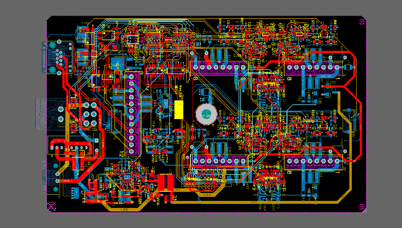
We have worked on many complex PCB Layout designs that required many layers and multiple signaling standards. These circuit boards almost always have high speed interfaces like SATA 6G, 10G Ethernet, XAUI, Fibre Channel, etc. They also usually have 2000+ components and nets in tight packaging. During the layout of these types of designs we will bring in all schematics for the entire system to make sure all signals from board to board match up and perform without issues. For systems with a stack of boards, we will also import the mechanical step files of each placed board to insure there are no mechanical interferences between boards.
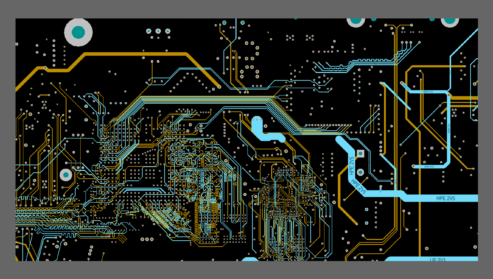
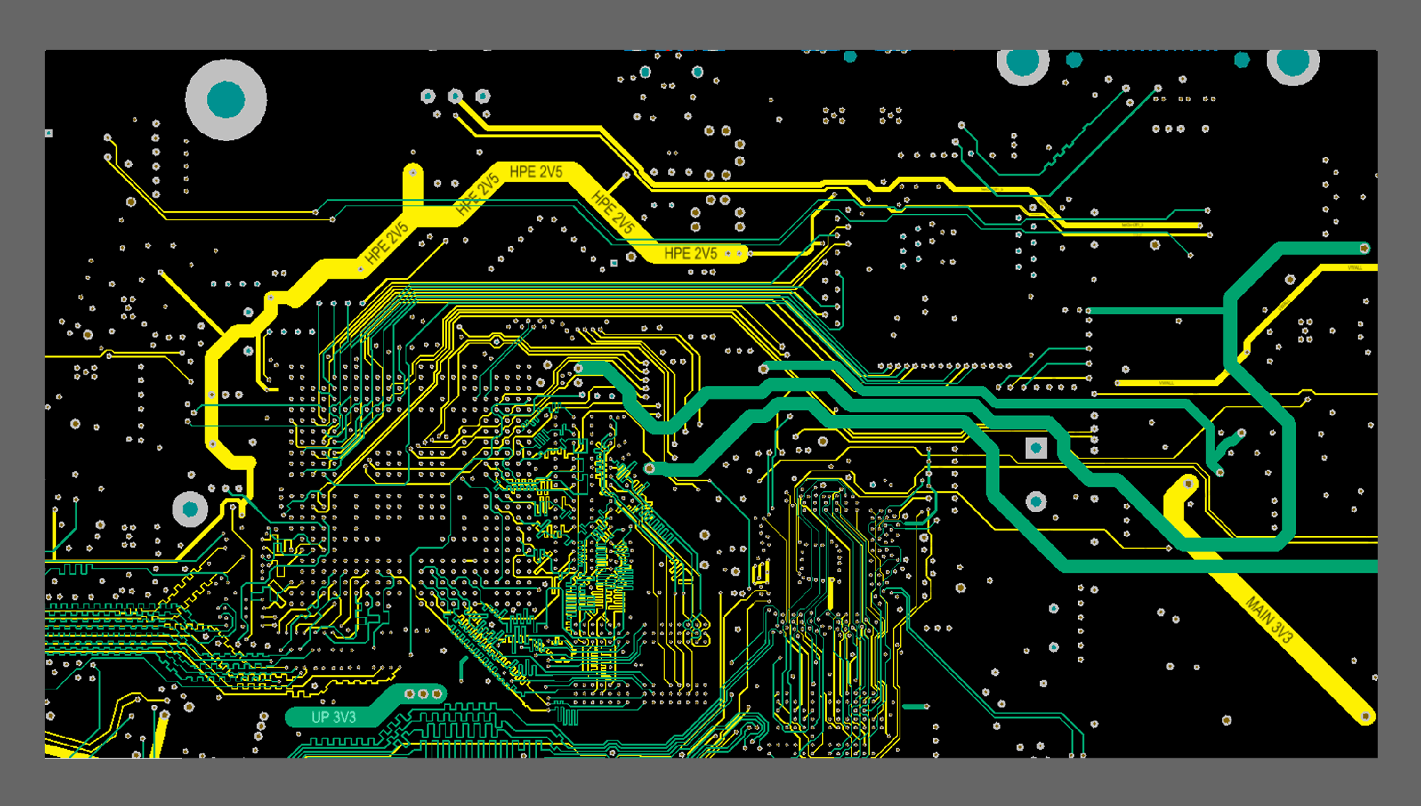
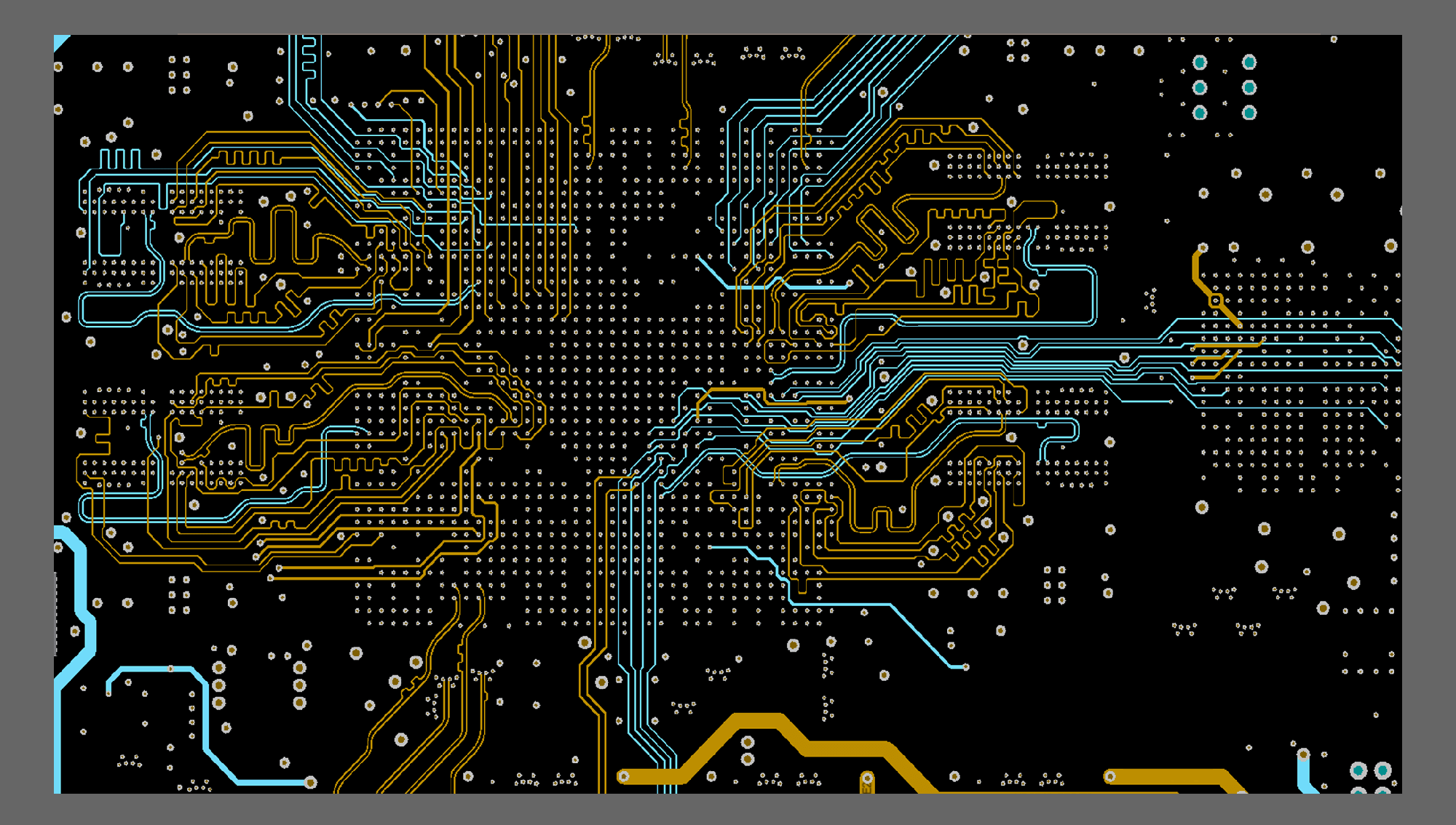
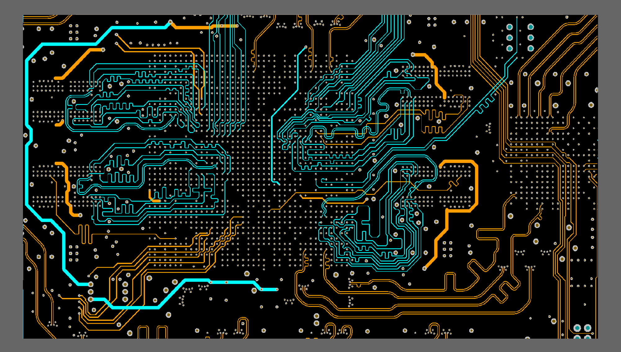
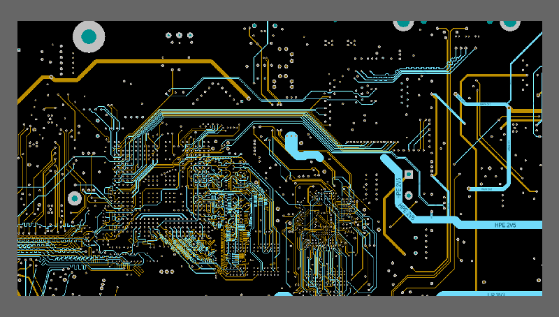
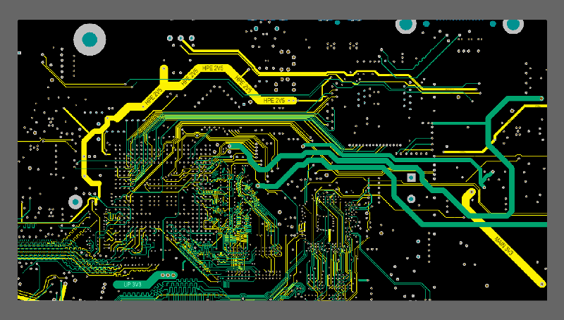
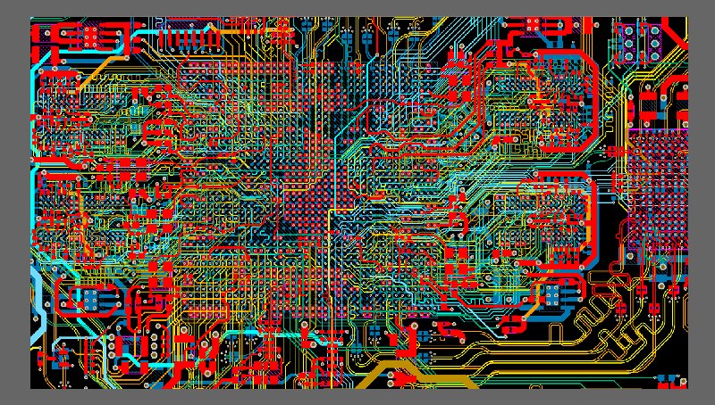
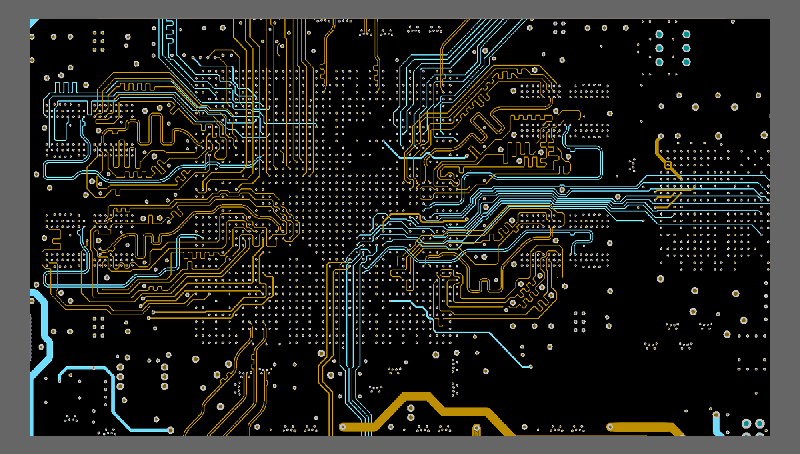
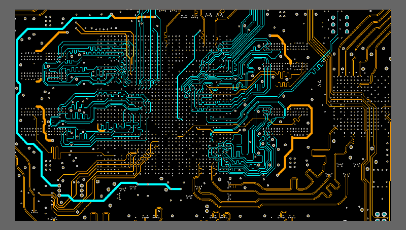
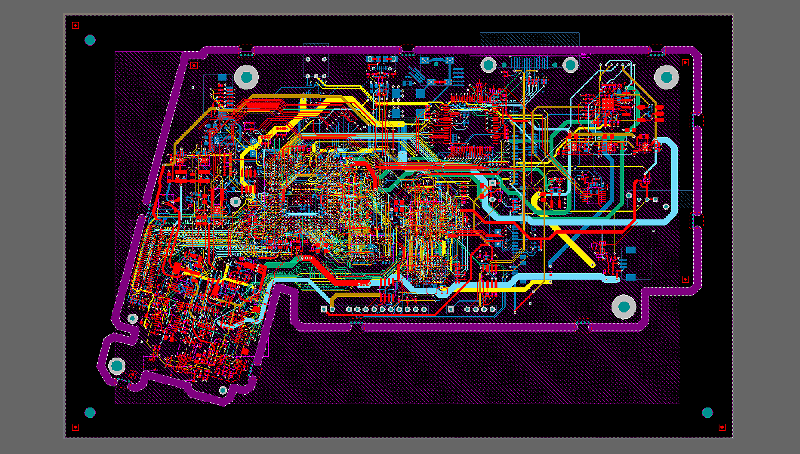
We have worked on many High Speed PCB layouts that required many layers & multiple signaling standards. These boards commonly have a mix of SATA 6G, 10G Ethernet, and many DDR3/DDR4 running at full speed. These designs also usually have large FPGA's and Processors and dense routing and placement. We can typically get these designs finished within 16 layers or less. During the high speed design process we will confirm that all design rules are imported correctly from the schematics and that they match up with the current signaling standard used. We will also insure that there are minimal parallel traces between adjacent layers. During this process we will ensure all necessary length tuning, controlled impedance, via back-drilling, etc are applied to maintain signal integrity of the high speed lines.
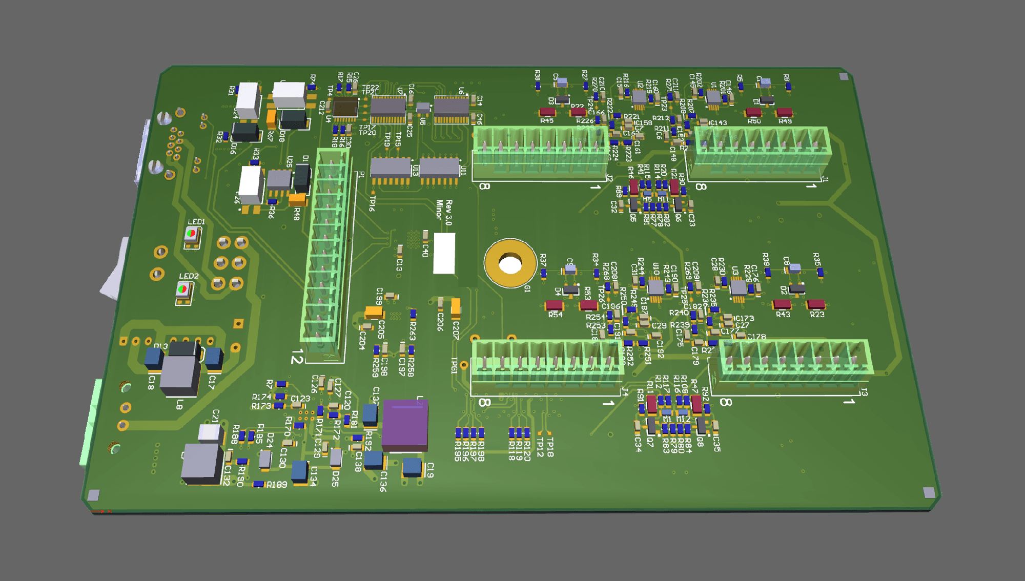
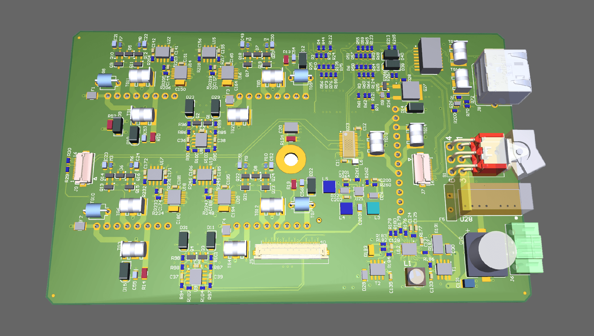
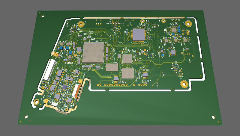
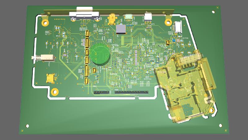
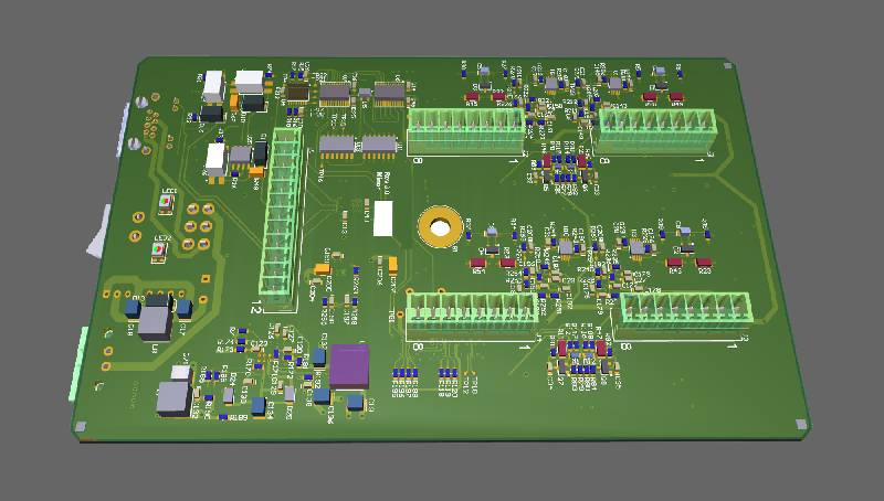
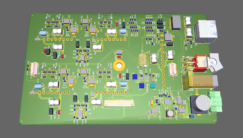
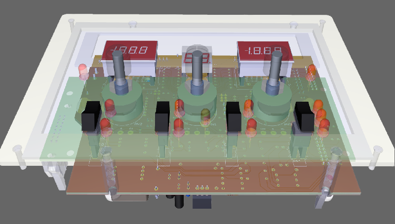
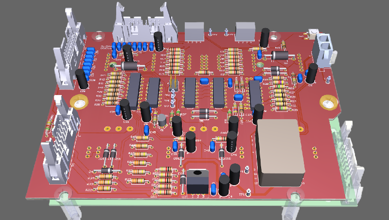
We have worked on many mechanically complex PCB Layouts that required importing multiple 3D models for interference checking. Some of these designs also used a non-standard placement rotation to achieve a perfect fit. Often These PCB Layouts have complex shapes and tight clearances between the layout and the housing.
We can also provide a quick turn time for standard PCB Layouts that don't have a lot of High Speed signaling or complex mechanical constraints. These designs are usually less than 10 layers and don't contain many large FPGAs, CPUs, DDR or complex signaling.
Single sided to
18+ Layers
Rules Driven PCB Layout Designs
Full Documentation Package
Fast Turn Times
(DFM) Design for Manufacturing
Large PCB designs 5000+ component / nets
True 3D design
.STEP file import for PCB constraints
3D PDF Generation
Fully Hand Routed
SMT, Through Hole, & Mixed
(DFT) Design for Test
High Frequency RF & Microwave PCBs
High Speed Digital
Precision Analog
Mixed Analog & Digital
Audio & Video
High Current & High Voltage
Multiple board systems
Mother Board Design
Ultra High Speed (10G+)
Differential Routing
Controlled Impedance
Length Matching
High Pin Count BGAs
Embedded Transformers
Signal Integrity
High Speed Backplane
Ultra High Density
Blind Vias & Buried Vias
Micro Vias
Micro BGA
HDI PCB Designs
EMI/EMC Sensitive Designs
Flex Circuits
Rigid Flex boards
Via Back-drilling
Cyclone III, IV, V
Stratix III, IV, V, 10
Arria II, V, 10, GX
Spartan 6, 7
Artix 7, UltraScale
Kintex 7, UltraScale
Virtex 7, UltraScale
Zynq, UltraScale
RTG4
RTAX-S/SL
RTAX-DSP
RTAX-SU
RT ProASIC3
iMX6, iMX7, iMX53
Kinetis MCU
Cortex-M MCU
Vitesse
Caracal-1/2
SparX-IV
E-StaX-IV
Aquantia
AG2104 - 10G PHY
AG2403 - 10G PHY
AQR105 - 1G/10G
AQR405 - 1G/10G
DDR2, DDR3, DDR4
eMMC Flash
NOR/NAND Flash
High Speed SRAM
RLDRAM
QDR II / II+
LPDDR2 / LPDDR3
C6000 DSP Series
C6000 DSP + ARM
C5000 DSP Series
DaVinci & OMAP
SigmaDSP
TigerSHARC
Blackfin Processor
1G, 10G Ethernet
2G, 4G, 8G, 16G FC
SATA I, II, III
USB 2.0, 3.0
PCIe 1.0-4.0 (16G)
FireWire
SGMII
RGMII
HDMI
SERDES
LVDS
XAUI / XGMII
10G-KR
We will provide all manufacturing files required to have your PCB layout built at any facility.
Gerber
NC Drill
ODB++
Fabrication Drawing .PDF
IPC Test point report
We will provide the following files for automated parts placement.
X,Y Centroid file in both formats
(.txt, .csv)
Assembly Drawing .PDF
Assembly standard 3D views
We will provide the following files for mechanical verification of the PCB design.
3D .step
3D .IDF
3D PDF
We will provide all standard Altium design and library files.
.PcbDoc
.PrjPCB
.OutJob
.DsnWrk
.SchDoc
.SchLib
.PcbLib
ADDRESS
3161 Meadowbrook Pl.
Dacono, Colorado 80514
CONTACTS
Email: info@hytek-ed.com
Email: sales@hytek-ed.com
Phone: 888-683-2950